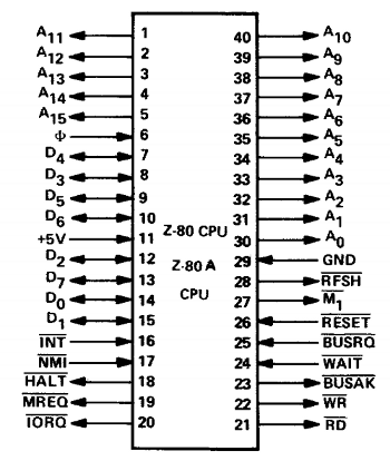
interfacing to the Z80 is SO EASY!
(image is from
Ken Shirriff's blog: Why the Z-80's data pins are scrambled
- all signals are not multiplexed, easy to use
- signals interface directly with RAM, ROM chips
thus inverted logic for read or write
- 16 address lines, thus 64k
- 8 data lines, thus being an 8 bitter
- status lines
The Z80 won for its ease of integration.
Many hobbyists breadboarded it
because a minimal system is only 3-4 chips:
CPU, ROM, interface chip, maybe RAM.
Very little glue logic was required,
just address decode and clock.
NO chip required for clock gen, interrupt handler
or bus buffering/latching mux signals.
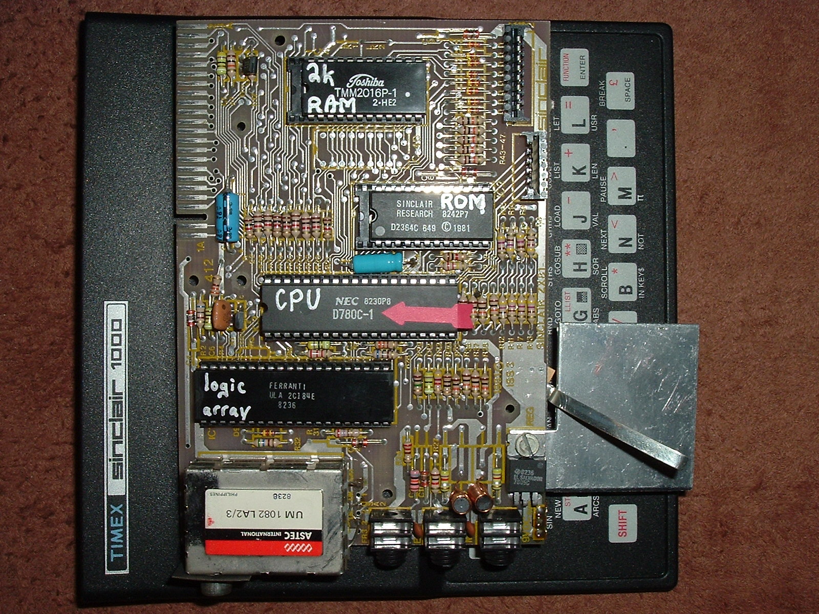
The Timex/Sinclair 1000 was only 4 chips:
CPU, RAM, ROM,
Uncommitted Logic Array (ULA)
This was accomplished by
generating the video in software!
Z80 bus states
             M1  MREQ  IOREQ  RD  WR  RFSH
instr-fetch  X   X            X
refresh          X                    X
memory read      X            X
memory write     X                X
I/O IN                  X     X
I/O OUT                 X         X
int ack      X          X
There is a "gotcha": the memory read timing
allows only 1 1/2 cycles for opcode fetch,
2 cycles for memory read or write,
thus requring memory speeds of:
MHz	1	1.5	2 cycles in nS
 4	250	375	500
 6	166	250	333
 8	125	188	250
10	100	150	200
20	 50	 75	100
The STD bus was originally the Z80 signals
as an industrial standard for embedded industrial control systems.
It was later expanded to other CPUs and more memory.